>> I am blown away by the wafer of Xbox 360 CPUs hanging on this guy's wall. That was a kingly gift!
Yeah, the only place I've seen a full wafer on display is a display case in the lobby of a chip company office building. I wonder how often some process goes out of whack and they get an entire known-bad wafer that still looks great?
You can buy complete wafers on ebay for a few bucks, so I'd guess it's pretty common.
I think many of the alignment steps during manufacturing involve making a wafer, seeing how misaligned it is using an electron microscope, adjusting all the machines, then making another wafer. Repeat until the wafers start working.
"Wafer of the Sony PlayStation 1 CPU. While decaping a Sony CXD8606Q, I was very lucky to be able to match the die to an unidentified wafer I had in my collection. The 6“ wafer could accommodate a total of 200 individual dies."
The manufacturing pipeline is generally pretty long too, and you can stop wafers midflight if you're just going to throw them out anyway. So for instance, if you have some B0 wafers that have enough metal layers that you couldn't easily change them into B1 wafers half way through the process, you might end up with it being cheaper to end up with unusable wafers for plaques and what have you. The fab is generally happy to have the extra capacity even for tail end of the design. There's generally some cheap customers that'll slot in wherever there's gaps.
It was always rumored around the FAB that dropping a case of wafers was akin to totaling a Ferrari. Maybe ~20 wafers in a case, so this math checks out!
They always have rejects. Actually, that's almost certainly an unfinished wafer. Modern flip chips don't look like that finished - you have an array of pads and power distribution covering all the cool features.
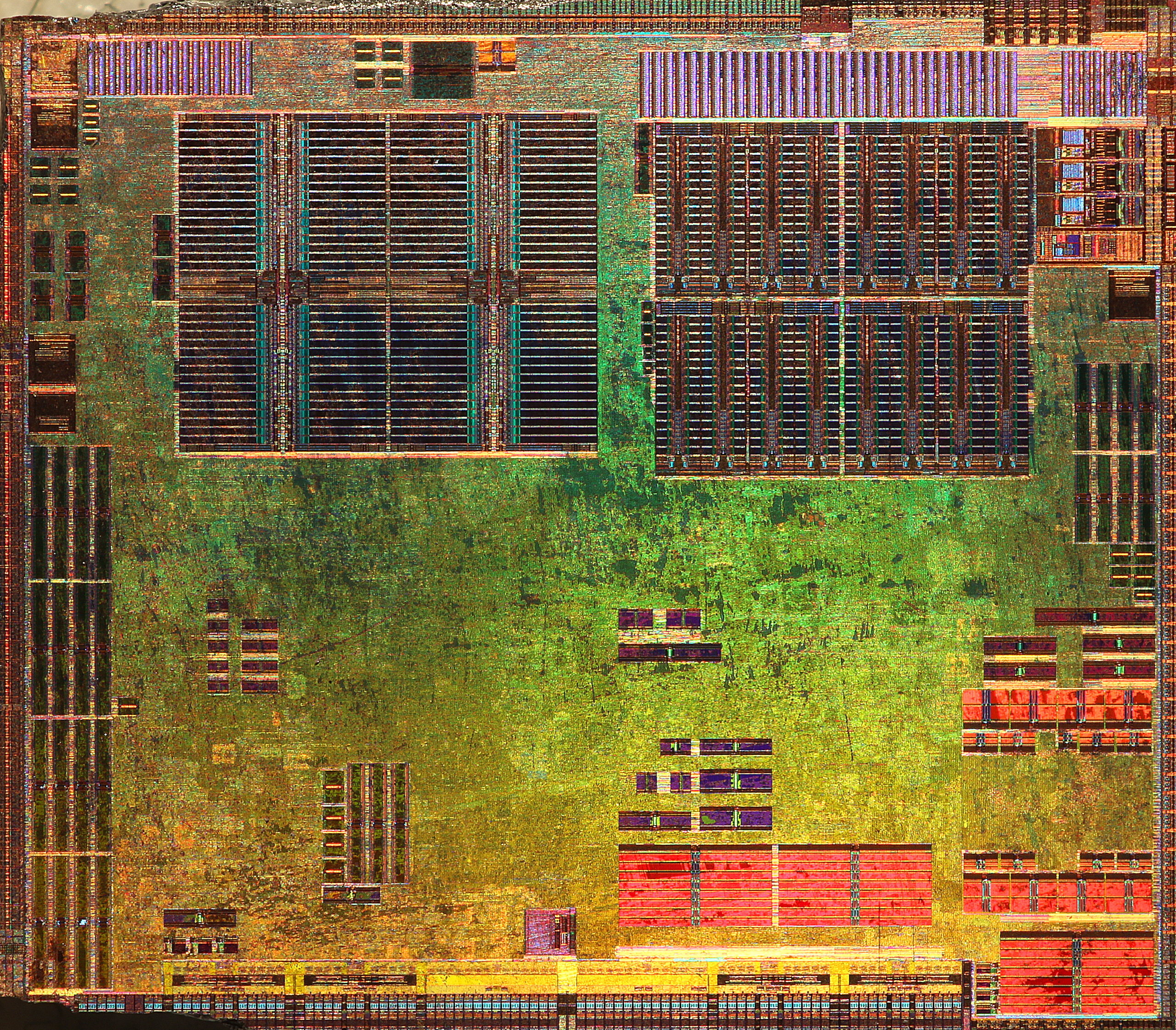
I think there's a good chance that wafer doesn't have any metal layers, or only M1 at most. It looks the same as the chips I've delayered and removed all or almost all of the metal layers from. For example, here's a shot of the Wii's GPU with the metal layers scraped off: